Recently I decided to dust off my old ZX81, the very machine that I learned programming on some 30+ years ago. It’s getting kind of difficult to find a TV that works with it, especially as I have the 1st ULA version that didn’t do the sync signals correctly. So I decided to “invest” (it’s only 10€!) into a ZX8-CCB (Crystal Clear picture Basic). It is a small additional PCB that provides an FBAS output with much cleaner signals.
The only question was the placement, in pretty much all pictures its fitted with long wires somewhere in the enclosure or in a gutted modulator. For preservational reasons I didn’t want to completely empty out the modulator but still wanted to use its output connector. So I came up with this placement that I haven’t seen before but makes for very neat cabling (using a simple PowerStrip to hold the PCB):
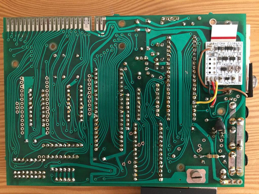
Bottom view
Detailed bottom view
From the top you basically don’t see anything except the small brown cable that goes into the unused hole in the modulator housing to the connector (the original modulator connection just being unsoldered but left intact).
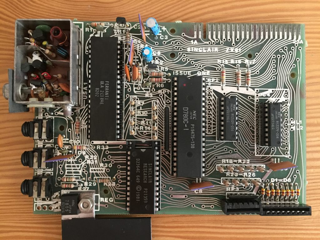
Top view, nothing really visible
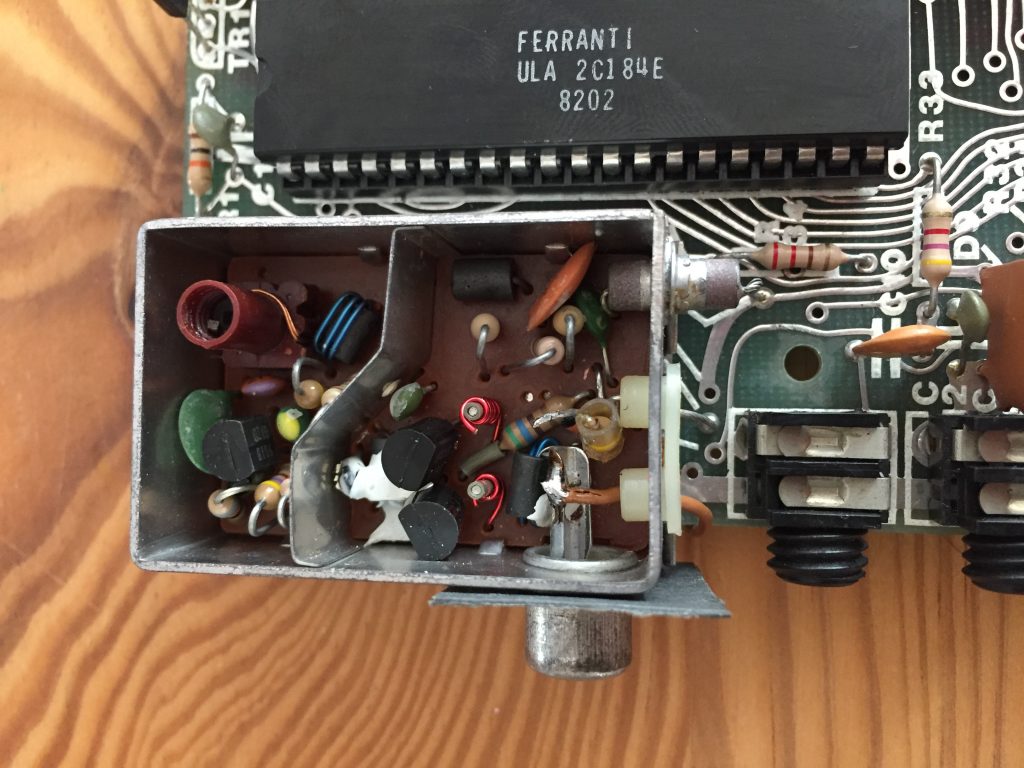
Detailed view of modulator
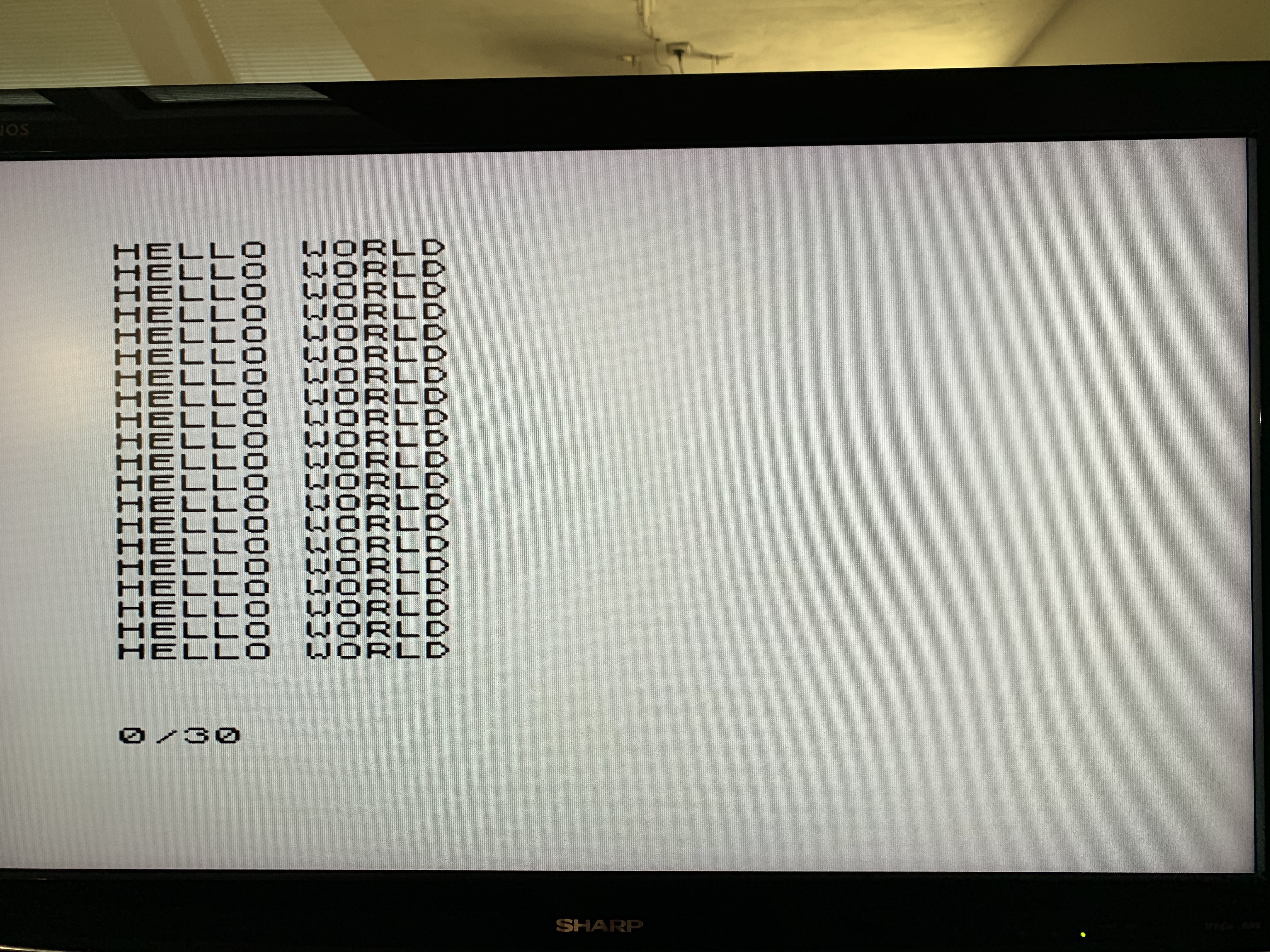
At first it didn’t show any picture. Even though it says that it comes pre-adjusted for the 1st edition ULA mine was apparently sufficiently different that the picture remained black. But not to worry, after playing with the two small potentiometers the screen came to life and voilà, the ZX81 now outputs a clean picture:
The QL and its non-standard video interface has always been a problem, even more so since the introduction of LCD monitors. Since I got my QL out of storage a few years ago I’ve been looking for a solution. I bought all kinds of Chinese video converters, the GBS8220 for example produced a very unstable picture for me. The small black HDMI converter without a name worked a lot better, but here pixels went missing on the left side. Only a small adjustment would be needed, but the manufacturer has filed off all chip markings, making modifications even more difficult.
One and a halve year ago I tried to tackle the problem the only way a software guy like me could: with software. I took a Raspberry Pi, learned to program it without any operating system (“bare metal”) and connected it to the QL bus. The idea was to listen to any access to the screen memory and mirror an emulation of it on the HDMI output. This is what it looked like:
QL-PI HDMI adapter
It almost worked but there were problems with the address decoding GAL. With my knowledge today I probably could have solved it, but I also bought myself a Tetroid GoldCard later and it’s not exactly easy to get to the required bus signals when that is fitted, so the project was put on the back-burner.
Due to the mentioned GoldCard I also created a new version of the QL-SD device (as the original was incompatible) and for this I had to learn the Verilog hardware description language. A few months later I invested even more time to update the QL core for the MiSTer FPGA board (in progress and a tale for another time), also written in Verilog.
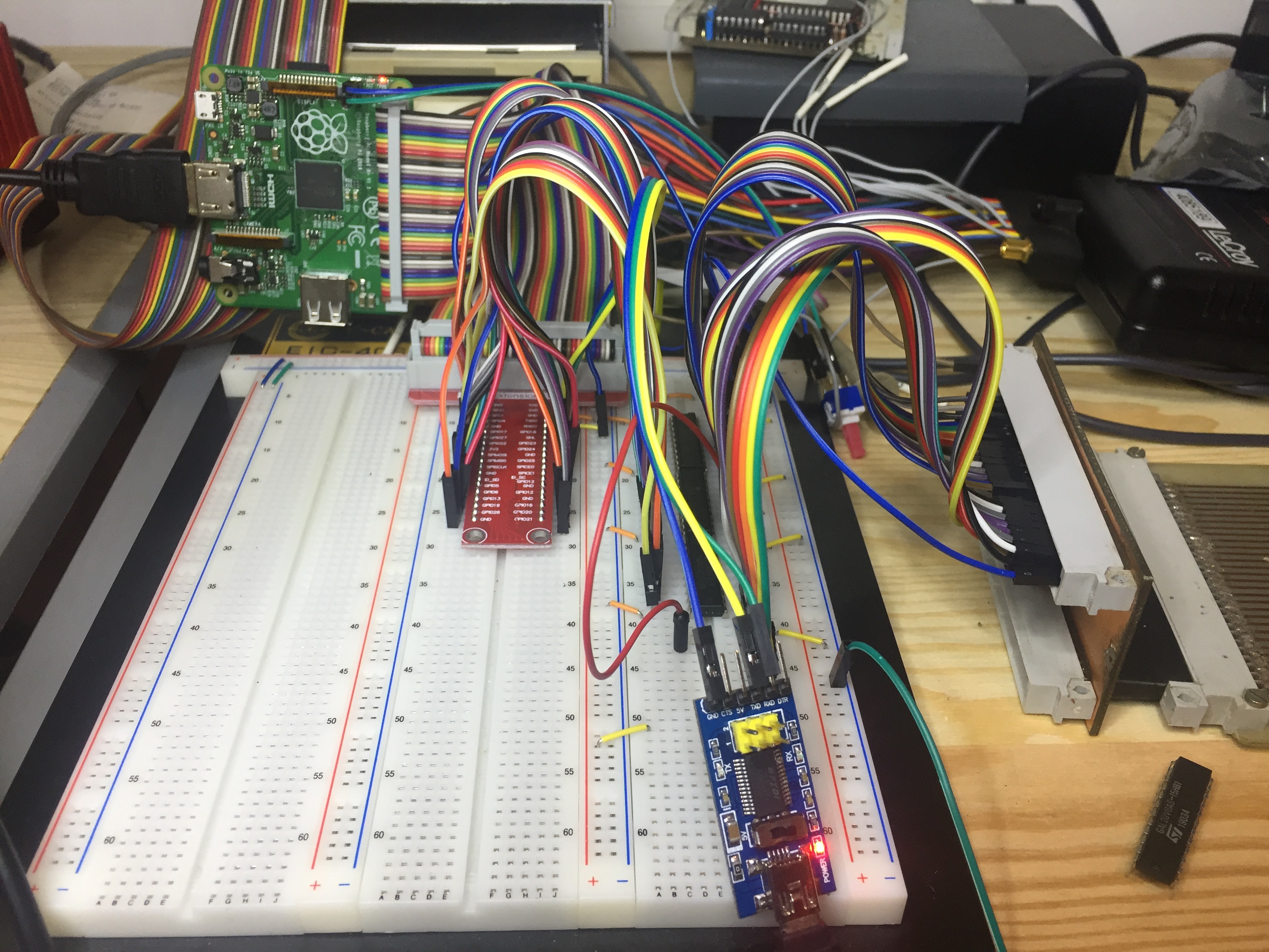
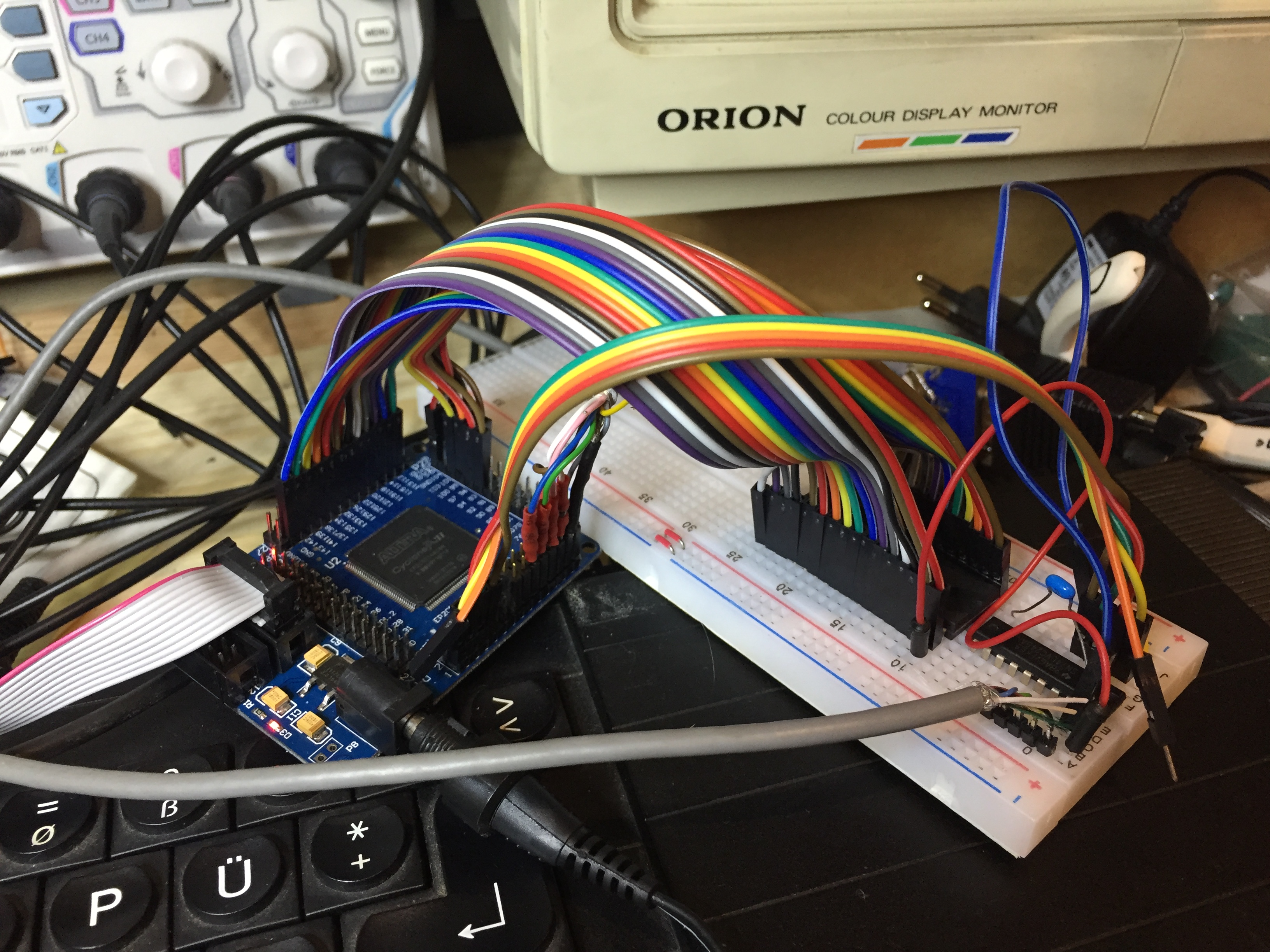
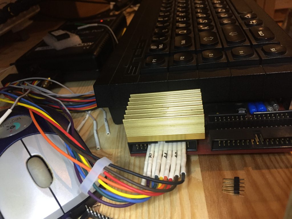
With this FPGA experience under my belt I revisited the display problem and tried another approach: using an old Cyclone II FPGA board plus some other chips I had laying around I managed to implement a QL-RGB -> VGA converter. It converts the 512×256 50Hz QL screen into a standard 1024×768 60Hz VGA signal that can be processed by probably every monitor in existence or further converted into HDMI if needed (the Cyclone II is too old to generate HDMI directly). This is what that looks like, a lot simpler than my previous approach:
FPGA based QL video converter
This is the very first prototype and it can actually only do mode 4: the SRAM I had in my bits-and-pieces box has an access time of 55ns. The VGA pixel clock is 65Mhz, meaning I need to generate a new pixel every 15ns. As pixels are doubled in x direction I need a new colour every 30ns. With 2 pixels per byte this means I need a new byte every 60ns. This would fit the requirement but the QL screen must also be captured and written to RAM at the same time! So currently it only works by packing 4 pixels into a byte, but this can easily be changed using a faster RAM chip.
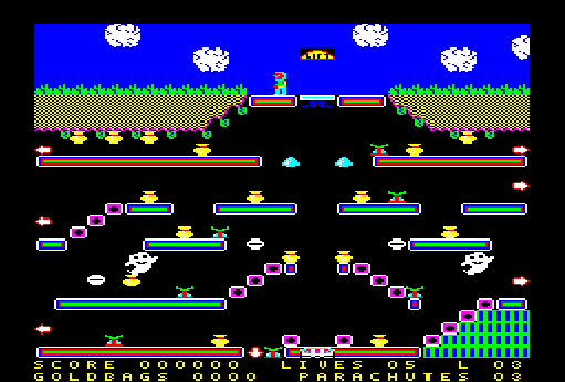
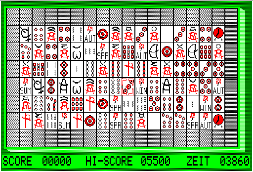
In the end the effort paid of, the picture is pleasantly rock steady and complete:
Next step is to order some faster RAM and create a PCB for it, but now that it finally works I can start sleeping at night again, so this might take a while 😉
When importing a project into Quartus 18.1 it helpfully suggests that it can rebuild the PLL IP blocks. Problem is, afterwards the MegaWizard doesn’t want to recognise the blocks anymore. It doesn’t even show an error, it just doesn’t do anything. As somebody who has never even used a MegaWizard before that was somewhat unfortunate.
Intel apparently wants to get rid of the Altera roots and the newly written block is called “PLL Intel FPGA IP” now instead of “Altera PLL”. Problem is, the MegaWizard doesn’t know about the new name. But it can be helped, just manually alter the file “pll_wizard.lst” in the “ip\altera\altera_pll” directory. Changes are in bold:
[Basic Functions|Clocks; PLLs and Resets|PLL]
PLL Intel FPGA IP v18.1= "%t" "%w/../common/lib/megawizard.pl" --wizard:altera_pll  --early_gen:on --wizard_file:"%w/source/top/pll_hw.tcl" --familyparameter:device_family %f %o %h
<INFO>
[...]
<PINPLAN SUPPORTED="ON"/>
<ALIAS>Altera PLL</ALIAS>
<ALIAS>Altera PLL v10.0</ALIAS>
<ALIAS>Altera PLL v10.1</ALIAS>
[...]
<ALIAS>Altera PLL v18.0</ALIAS>
<ALIAS>Altera PLL v18.1</ALIAS>
<ALIAS>PLL Intel FPGA IP v18.1</ALIAS>
<ALIAS>PLL Intel FPGA IP v19.0</ALIAS>
<ALIAS>PLL Intel FPGA IP v19.1</ALIAS>
<ALIAS>PLL Intel FPGA IP v20.0</ALIAS>
<ALIAS>PLL Intel FPGA IP v20.1</ALIAS>
</INFO>
Prompted by a customer request I have extended my QL-SD demo file with a few free QL games, 20 in total, including some that were never available for free before but for which I have the rights to release (basically the Jochen Merz catalog, thanks Jochen!).
I went to great length to try to make it as easy as possible, usually you can just select a game in the boot screen and it will run, everything is pre-configured. Even (Super)GoldCards are slowed down when necessary, still not every game will run properly on every QL configuration. The most compatible configuration is probably a QL with expanden memory but without any GoldCard.
Martyn Hill, while testing his brand new Tetroid SuperGoldCard clone, has discovered a strange bug where his QL crashed when he was loading a _scr file into the QL’s screen memory. It works fine without the SuperGoldCard. A lot of theories were put forward, like:
It’s a problem with the SuperGoldCard: turns out it works fine when QDOS or a very early Minerva version is used instead
It’s connected to the memory timing of the screen area: turns out is also happens in fast memory
It’s connected to the 68020 processor: turns out is also happens on the 68000 processor
The SuperGoldCard patches are wrong: I’ve analyzed all the patches and they all look fine. In fact the patch code is identical to Minerva’s code except for the timing loops. Still, it appeared to work with earlier versions of the patches, which makes it weird again.
Personally I couldn’t care less if Microdrives work or not and the fact that this bug was not discovered for so long strongly implies that most other people also don’t use Microdrives with SGC systems anymore. Still I have trouble resisting a good puzzle so I had a look. And then another one. And then ten more because this was a very elusive bug.
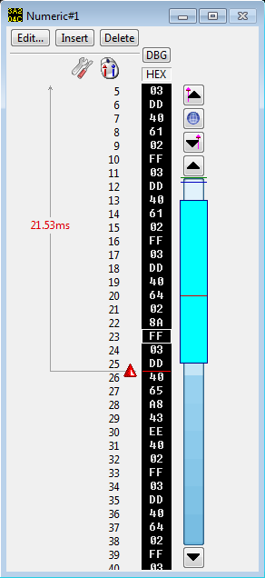
The problem is that not only is the bug located in ROM locations that are hard to debug anyway, the MDV code is so time critical that it’s impossible to step through the code. So how can one debug this? Hardware to the rescue! The SuperGoldCard very conveniently has a parallel port on board that can be accessed very simply by the software. By connecting a logic analyzer to all 8 data lines and sprinkling output commandos throughout the MDV code I can get a live trace of what the code is doing or output the contents of registers byte-by-byte.
Bytes output by the instrumented driver
In hindsight I should have found the problem much earlier because of the symptoms, but that’s easy to say after you know what’s going wrong. Let’s make a little quiz, here’s the code part with the problem and you can try to spot the bug:
        move.w  #blksize,d0     full block normally (512)
        cmp.b   lstblok(a0),d7  is it the last file block?
        bne.s   not_last        no - copy to end of it
        move.w  lstbyte(a0),d0  get the number of bytes in last block
not_last
        lsl.w   #blkbits-1,d7
        add.l   d7,d7           is it the first file block?
        lea     -md_deend(a1,d7.l),a5 where to put data normally
        bne.s   not_frst
        moveq   #md_deend,d1    yes - move on past the file header
        add.l   d1,a4
        add.l   d1,a5
        sub.w   d1,d0           copy fewer bytes
not_frst
        ror.l   #2,d0           long words, and save odd byte count
        bcc.s   unbf_dbr        carry means there is an odd word to do
        move.w  (a4)+,(a5)+     if so, do it
        bra.s   unbf_dbr
unbf_lop
        move.l  (a4)+,(a5)+     move a long word
unbf_dbr
        dbra    d0,unbf_lop
        add.l   d0,d0           see if there's an odd byte to go
        bpl.s   notabyte
        move.b  (a4)+,(a5)+     if so, do it
notabyte
Keep in mind that the code is not generally broken, it sometimes works! The problem also appears for the first block, so you can pretty much ignore the special handling of the last block. Found it? I’ll wait…
.
.
.
.
.
The “ror.l #2,d0” is a pretty clever way to both divide the register by 4 (because the copy loop does long words) while still remembering the odd bytes that also need to be copied. But it relies on one thing: that bits 16 and 17 of the register are zero. These bits are shifted into the lower 16-bits and are then used by the dbra instruction, which means that if they are set instead of copying 128 long words it will copy at least 16384. Talk about a buffer overflow!
You should now also see why it sometimes works. Remember earlier that I wrote “In fact the [MDV] patch code is identical to Minerva’s code except for the timing loops.”. The timing code in the original Minerva ROM is hidden behind a macro but in the end looks like this:
; For delays 5 to 19µs
        moveq #([us]*15-38)/4,d0        four byte sequence
        ror.l  d0,d0

; For delays 21 to 309µs
        moveq   #([us]*15-50)/36,d0     six byte sequence
        dbra    d0,*

; ... etc, other variants are similar
For the (S)GC this is exchanged by loops like this:
        move.w  gmt_fgap,d0              ; 2800 us
        dbra    d0,*
I guess everybody can see the difference now, the original code clears the upper word of D0 and the replacement code does not. And as it happens the upper word is $FFFF from an earlier call to md_slave. All in all a very subtle difference, hard to spot by just looking at the code.
The solution I chose is it to exchange the “move.w #blksize,d0” line with “move.l”. That adds two bytes (every byte is precious in Minerva, there are not many left!), but this is the minimum I can get away with without relying on side effects of outside code, which is how this bug was introduced in the first place.
As this is the second fix from me for Minerva 1.98 I will have to think about how to mark these modified Minerva versions as increasing the version number is a no-go unfortunately. 1.99 is the last number we can use in theory before running into extended compatibility problems and I’m not even sure about this, 1.98 is still a safer choice.
Anyway, I hope this was interesting to read, leave a comment if you want. I will soon release a fixed binary version.
The last few days I’ve spent way too much time analyzing the (Super)GoldCard boot ROM. The sources supplied along with SMSQ/E are only sparsely commented disassembly that was basically impossible to read. It irked me to no end that I didn’t understand the code and finally I did something about it. The process had a strange fascination like putting together a 10000 piece puzzle
Anyway, let’s begin. The ROM consists of three parts:
Address
Name
Contents
$0000-$7FFF
GOLD
FLP + RAM + TK2
$8000-$BFFF
PATCH
Patches + Basic extensions + PAR + network + DEV
$C000-$FFFF
BOOT
Boot/patch engine
GoldCard
On the Gold Card the memory map on boot looks like this:
Address
Contents
$0000-$BFFF
QDOS (read), RAM (write)
$C000-$FFFF
BOOT section of GC ROM
$10000-$17FFF
RAM
$18000-$1BFFF
QL hardware registers
$1C000-$1C0FF
GoldCard hardware registers
$1C100-$1FFFF
RAM
$20000-$3FFFF
128kb RAM (including VRAM)
$40000-$4FFFF
Complete GC ROM
QDOS boots normally, finds 128kb of RAM (because of the ROM) and executes the GC BOOT code at address $C000. This in turn initialises the hardware, copies and patches QDOS to RAM, copies parts of the GC ROM to RAM and finally issues another reset. This is why on the GoldCard the QL always boots two times.
Fun-fact: the GoldCard can boot without any firmware ROM, this makes it somewhat possible to inspect the above memory layout live.
After boot the memory map looks like this:
Address
Contents
$0000-$BFFF
Patched QDOS in RAM, write protected
$C000-$FFFF
ROM port extension
$10000-$17FFF
GOLD section of the GC ROM
$18000-$1BFFF
QL hardware registers
$1C000-$1C0FF
GoldCard hardware registers
$1C100-$1C1FF
GoldCard firmware variables
$1C200-$1FFFF
PATCH section of GC ROM
$20000-$1FFFFF
1920kb RAM (including VRAM)
SuperGoldCard
On the SuperGoldCard the memory map on boot looks a bit differently:
Address
Contents
$00000-$0FFFF
SGC ROM (read), RAM (write)
$10000-$17FFF
RAM
$18000-$1BFFF
QL hardware registers
$1C000-$1C0FF
SuperGoldCard hardware registers
$1C100-$1FFFF
RAM
$20000-$3FFFF
128kb RAM (including VRAM)
$40000-$4FFFF
Complete SGC ROM (again)
$50000-$3FFFFF
RAM
$400000-$40FFFF
QDOS ROM
In this case the SGC ROM doubles as the boot ROM and gets executed immediately. This is why the SGC does not need to double-boot. Again QDOS is copied and patched and parts of the SGC ROM are copied, too. Unlike with the GC, the copies of the SGC ROM are write protected.
Address
Contents
$0000-$BFFF
Patched QDOS in RAM, write protected
$C000-$FFFF
ROM port extension
$10000-$17FFF
GOLD section of the GC ROM, write protected
$18000-$1BFFF
QL hardware registers
$1C000-$1C0FF
SuperGoldCard hardware registers
$1C100-$1C1FF
SuperGoldCard firmware variables
$1C200-$1FFFF
PATCH section of SGC ROM, write protected
$20000-$27FFF
VRAM1, writes are mirrored to QL hardware
$28000-$2FFFF
VRAM2, writes are only mirrored if SCR2 is enabled
$30000-$3FFFFF
RAM
$400000-$40FFFF
QDOS ROM
$4C0000-$4FFFFF
Extended I/O area
Configuration
The (Super)GoldCard does not have any kind of RAM that survives without power but still can store a bit of configuration like if F1 should be automatically pressed on boot. Well, how can this be? This was some mayor kind of “heureka” effect while analyzing the code. The cards contain a realtime clock chip that does not possess any additional RAM either, but it has a register that controls the interrupt line. The interrupt is never used on the golden cards, so the firmware just (ab-)uses the 4-bits available to store the configuration! Really clever.
Patches
The topic of what kind of patching the cards do on boot is almost mythical and was basically the reason I started this in the first place. All patches have been decoded and commented and everybody can look at them now (download below). There are a few patches that remove the most common bugs from the original QDOS ROM and a lot more that are applied to every ROM including Minerva. In some cases bugs in Minerva have been patched, but in these cases they have also been fixed in Minerva, so they usually don’t get applied anymore. One huge part is replacement of the MDV, network and I2C code, as these are all very timing critical.
Most remaining patches are exclusive to SGC because of the added code cache handling and the difference in exception frames of the 68020 to the 68000. Also there is an emulator for the “MOVE SR,x” instruction that became privileged on later processors.
The Masterpiece
Quite many of the patches actually alter QDOS for use with a graphics card with more resolution. At first I thought this was somehow connected to the Aurora and wondered why the condition for their activation apparently could never be true. But then I saw that Aurora’s VRAM starts at $4C0000 and the patches are all for VRAM that starts at $4E0000. The only explanation is that this is all for Miracle Systems never release Masterpiece graphics card. They must have been pretty well along the development path if these patches all made their way into the default ROM already. It even goes so far as to patch PTR_GEN after it is loaded.
The interesting thing about this is that the patches could easily be altered to work with the Aurora. As I don’t own an Aurora this is not for me to do, however.
The code
Finally here is the source code for all to see. For this version it was important to me that the result is bit-identical to the original source code, even though I had a strong urge to to change some code along the way… The result is not completely bit-identical to the GC2.49 ROM, but mostly because the utility libraries have changed. I have verified that the patches are exactly the same.
I will also submit the changes to Wolfgang to incorporate back into the SMSQ/E source code.
The QL-SD driver seems to be finished (note that it currently doesn’t work with the MiST FPGA board, but there are no more known problems with either the original QL hardware or the MiSTer FPGA machine).
Now the boring part has begun, which means hours of reading tax related stuff (selling stuff internationally is hard!), writing/updating the manual, preparing an order page, preparing shipping labels, etc. I really don’t enjoy this part of the process.
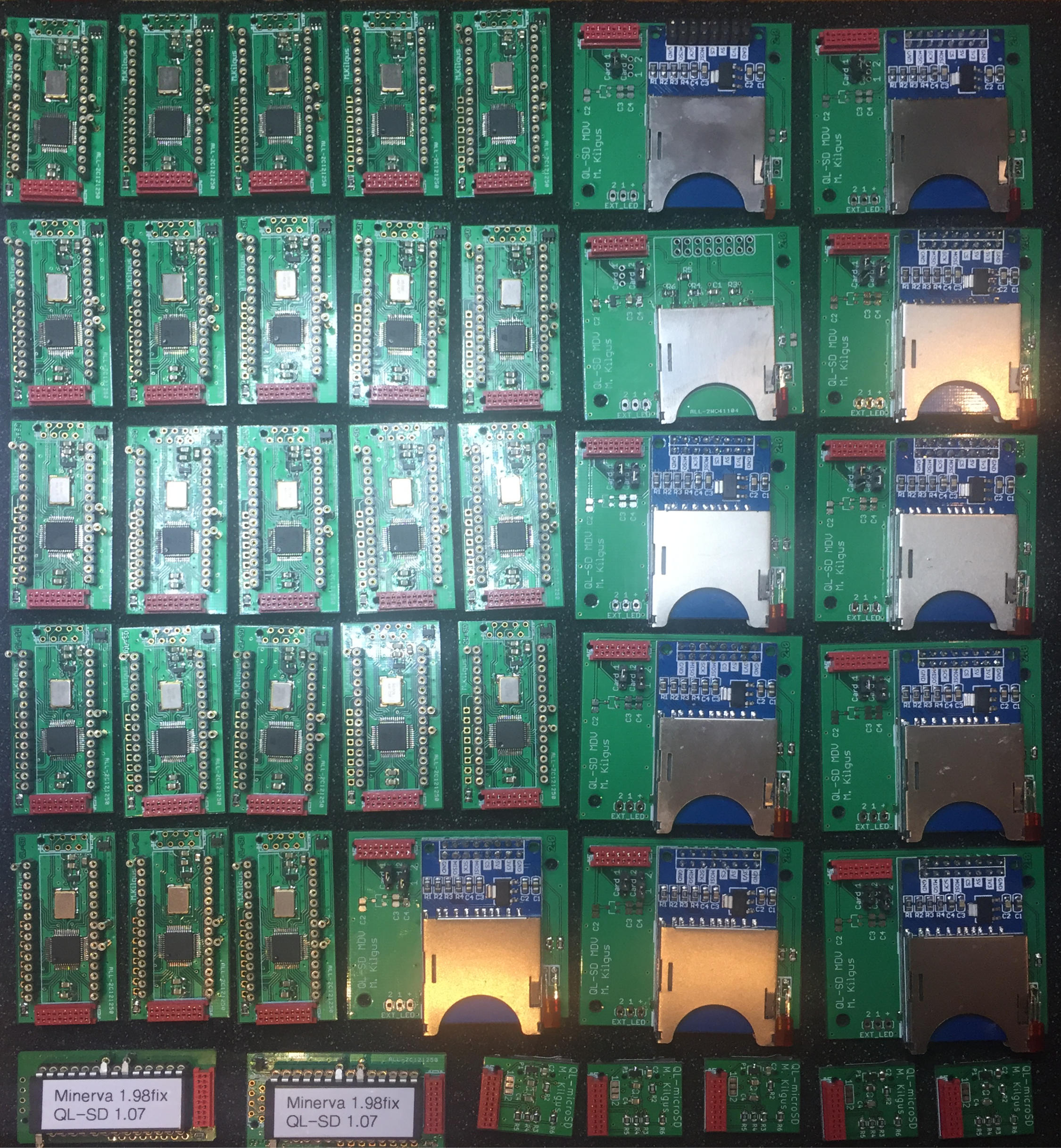
Anyway, as a short teaser, the hardware does exist now in some quantities:
I will probably open the order page publicly starting September, after my holiday.
Update: the old code had a bug if the EXE was made resident using the HOT_RES keyword (thanks to Jan Bredenbeek for pointing it out), updated code below.
Today I’ve had a short discussion about creating a QDOS executable that can both be LRESPRed (to install a thing) and EXecuted (to, erm, execute it). One important detail is that LRESPR must only work in the main BASIC, as otherwise the system will crash once the daughter BASIC is terminated. There are several ways to do it, but I’d like to share mine:
base    bra.s   start
        nop
        nop
        dc.w    $4AFB
        dc.w    4
        dc.b    'Test'

start
; Trick: on an EXE call a6 must point to either a BRA ($60) or JMP ($4E).
; both have bit 6 set ($40). On Basic a6 points to the MSB of sb_buffb.
; Bit 6 will never be set as long as QLs have less than 1GB of RAM :-)
        btst    #6,(a6)
        beq.s   lrespr                  ; Definitely LRESPR
        cmp.w   #$4afb,6(a6)            ; This check is somewhat optional...
        beq.s   job_start               ; but in case QLs ever have >1GB... :)

lrespr
        moveq   #sms.info,d0
        trap    #1
        tst.l   d1                      ; Job ID = main BASIC
        beq.s   basic_start

; LRESPRed from daughter SBASIC/MultiBasic
        moveq   #err.nimp,d0
        rts

; LRESPred from main BASIC
basic_start
;       ...
        moveq   #0,d0
        rts

; EXECed as normal job
job_start
;       ...